- 您现在的位置:买卖IC网 > Sheet目录17353 > ADR431BRMZ (Analog Devices Inc)IC VREF SERIES PREC 2.5V 8MSOP
�� ��
��
��ADR430/ADR431/ADR433/ADR434/ADR435/ADR439�
�THEORY� OF� OPERATION�
�The� ADR43x� series� of� references� uses� a� reference� generation�
�technique� known� as� XFET� (eXtra� implanted� junction� FET).�
�This� technique� yields� a� reference� with� low� supply� current,� good�
�thermal� hysteresis,� and� exceptionally� low� noise.� The� core� of� the�
�XFET� reference� consists� of� two� junction� field-effect� transistors�
�The� ADR43x� family� of� references� is� guaranteed� to� deliver� load�
�currents� to� 10� mA� with� an� input� voltage� that� ranges� from� 4.1� V�
�to� 18� V.� When� these� devices� are� used� in� applications� at� higher�
�currents,� use� the� following� equation� to� account� for� the�
�temperature� effects� due� to� the� power� dissipation� increases:�
�(JFETs),� one� of� which� has� an� extra� channel� implant� to� raise� its�
�T� J� =� P� D� ×� θ� JA� +� T� A�
�(2)�
�pinch-off� voltage.� By� running� the� two� JFETs� at� the� same� drain�
�current,� the� difference� in� pinch-off� voltage� can� be� amplified� and�
�used� to� form� a� highly� stable� voltage� reference.�
�The� intrinsic� reference� voltage� is� around� 0.5� V� with� a� negative�
�temperature� coefficient� of� about� ?120� ppm/°C.� This� slope� is�
�essentially� constant� to� the� dielectric� constant� of� silicon� and� can�
�be� compensated� closely� by� adding� a� correction� term� generated�
�in� the� same� fashion� as� the� proportional-to-temperature� (PTAT)�
�term� used� to� compensate� band� gap� references.� The� primary�
�advantage� of� an� XFET� reference� is� its� correction� term,� which� is�
�~30� times� lower� and� requires� less� correction� than� that� of� a� band�
�gap� reference.� Because� most� of� the� noise� of� a� band� gap� reference�
�where:�
�T� J� and� T� A� are� the� junction� and� ambient� temperatures,� respectively.�
�P� D� is� the� device� power� dissipation.�
�θ� JA� is� the� device� package� thermal� resistance.�
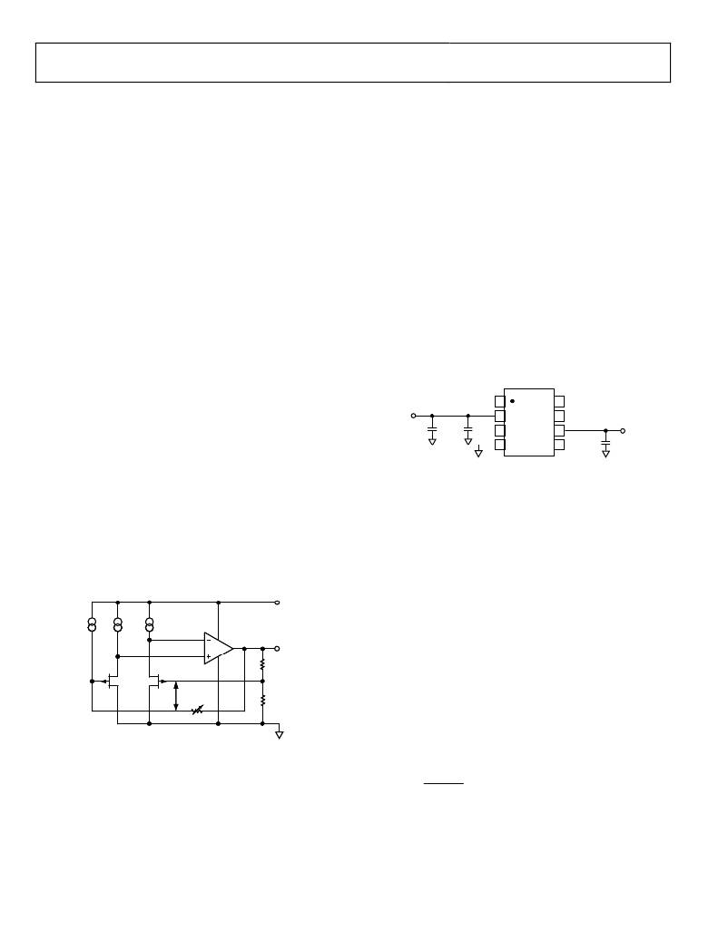
�BASIC� VOLTAGE� REFERENCE� CONNECTIONS�
�Voltage� references,� in� general,� require� a� bypass� capacitor�
��illustrates� the� basic� configuration� for� the� ADR43x� family�
�of� references.� Other� than� a� 0.1� μF� capacitor� at� the� output� to�
�help� improve� noise� suppression,� a� large� output� capacitor� at�
�the� output� is� not� required� for� circuit� stability.�
�TOP� VIEW�
�(Not� to� Scale)�
�comes� from� the� temperature� compensation� circuitry,� the� XFET�
�results� in� much� lower� noise.�
��temperature� correction� term� is� provided� by� a� current� source�
�V� IN�
�10μF�
�+�
�0.1μF�
�TP�
�NC�
�GND�
�1� 8�
�2� ADR43x� 7�
�3� 6�
�4� 5�
�TP�
�COMP�
�V� OUT�
�TRIM�
�0.1μF�
�with� a� value� designed� to� be� proportional� to� absolute� temperature.�
�The� general� equation� is�
�V� OUT� =� G� (� ΔV� P� –� R1� ×� I� PTAT� )�
�where:�
�G� is� the� gain� of� the� reciprocal� of� the� divider� ratio.�
�(1)�
�NOTES:�
�1.� NC� =� NO� CONNECT�
�2.� TP� =� TEST� PIN� (DO� NOT� CONNECT)�
�Figure� 30.� Basic� Voltage� Reference� Configuration�
�NOISE� PERFORMANCE�
�Δ� V� P� is� the� difference� in� pinch-off� voltage� between� the� two� JFETs.�
�I� PTAT� is� the� positive� temperature� coefficient� correction� current.�
�ADR43x� devices� are� created� by� on-chip� adjustment� of� R2� and� R3� to�
�achieve� 2.048� V� or� 2.500� V,� respectively,� at� the� reference� output.�
�V� IN�
�I� 1� I� 1�
�I� PTAT� ADR43x�
�V� OUT�
�R2�
�*�
�The� noise� generated� by� the� ADR43x� family� of� references� is�
�typically� less� than� 3.75� μV� p-p� over� the� 0.1� Hz� to� 10.0� Hz� band�
�for� ADR430,� ADR431,� and� ADR433.� Figure� 22� shows� the� 0.1� Hz�
�to� 10.0� Hz� noise� of� the� ADR431,� which� is� only� 3.5� μV� p-p.� The�
�noise� measurement� is� made� with� a� band-pass� filter� made� of� a�
�2-pole� high-pass� filter� with� a� corner� frequency� at� 0.1� Hz� and� a�
�2-pole� low-pass� filter� with� a� corner� frequency� at� 10.0� Hz.�
�HIGH� FREQUENCY� NOISE�
�The� total� noise� generated� by� the� ADR43x� family� of� references� is�
��?� V� P�
�R1�
�R3�
�shows� the� wideband� noise� from� 10� Hz� to� 25� kHz.� An� internal� node�
�of� the� op� amp� is� brought� out� on� Pin� 7,� and� by� overcompensating�
�the� op� amp,� the� overall� noise� can� be� reduced.�
�*EXTRA� CHANNEL� IMPLANT�
�V� OUT� =� G(� ?� V� P� –� R1� ×� I� PTAT� )�
�Figure� 29.� Simplified� Schematic� Device�
�GND�
�This� is� understood� by� considering� that� in� a� closed-loop�
�configuration,� the� effective� output� impedance� of� an� op� amp� is�
�Power� Dissipation� Considerations�
�R� O� =�
�r� O�
�1� +� A� VO� β�
�(3)�
�where:�
�R� O� is� the� apparent� output� impedance.�
�r� O� is� the� output� resistance� of� the� op� amp.�
�A� VO� is� the� open-loop� gain� at� the� frequency� of� interest.�
�β� is� the� feedback� factor.�
�Rev.� J� |� Page� 16� of� 24�
�发布紧急采购,3分钟左右您将得到回复。
相关PDF资料
GEM28DTAD-S189
CONN EDGECARD 56POS R/A .156 SLD
ADR435BRMZ
IC VREF SERIES PREC 5V 8-MSOP
RBM08DTBN
CONN EDGECARD 16POS R/A .156 SLD
RBM08DTBH
CONN EDGECARD 16POS R/A .156 SLD
ZXRE1004DN8TA
IC VREF SHUNT PREC 1.22V 8-SO
B82559A0501A013
INDUCTOR POWER .50UH 30A SMD
EBM22DTBN-S189
CONN EDGECARD 44POS R/A .156 SLD
MIC2549A-1BM
IC SW CURR LIMIT HI SIDE 8-SOP
相关代理商/技术参数
ADR431BRMZ-R7
功能描述:IC VREF SERIES PREC 2.5V 8MSOP RoHS:是 类别:集成电路 (IC) >> PMIC - 电压基准 系列:XFET® 标准包装:2,000 系列:- 基准类型:旁路,可调节,精度 输出电压:1.24 V ~ 16 V 容差:±0.5% 温度系数:- 输入电压:1.24 V ~ 16 V 通道数:1 电流 - 阴极:100µA 电流 - 静态:- 电流 - 输出:20mA 工作温度:-40°C ~ 85°C 安装类型:通孔 封装/外壳:TO-226-3、TO-92-3(TO-226AA)成形引线 供应商设备封装:TO-92-3 包装:带卷 (TR)
ADR431BR-REEL7
功能描述:IC VREF SERIES PREC 2.5V 8-SOIC RoHS:否 类别:集成电路 (IC) >> PMIC - 电压基准 系列:XFET® 标准包装:3,000 系列:- 基准类型:旁路,精度 输出电压:5V 容差:±0.5% 温度系数:100ppm/°C 输入电压:- 通道数:1 电流 - 阴极:80µA 电流 - 静态:- 电流 - 输出:15mA 工作温度:-40°C ~ 85°C 安装类型:表面贴装 封装/外壳:TO-236-3,SC-59,SOT-23-3 供应商设备封装:SOT-23-3 包装:带卷 (TR) 其它名称:LM4040CIM3-5.0MLTRLM4040CIM3-5.0MLTR-ND
ADR431BRZ
功能描述:IC VREF SERIES PREC 2.5V 8-SOIC RoHS:是 类别:集成电路 (IC) >> PMIC - 电压基准 系列:XFET® 标准包装:3,000 系列:- 基准类型:旁路,精度 输出电压:3V 容差:±0.5% 温度系数:100ppm/°C 输入电压:- 通道数:1 电流 - 阴极:82µA 电流 - 静态:- 电流 - 输出:15mA 工作温度:-40°C ~ 85°C 安装类型:表面贴装 封装/外壳:6-TSSOP(5 引线),SC-88A,SOT-353 供应商设备封装:SC-70-5 包装:带卷 (TR) 其它名称:296-20888-2
ADR431BRZ
制造商:Analog Devices 功能描述:REFERENCE VOLTAGE:2.5V
ADR431BRZ-REEL7
功能描述:IC VREF SERIES PREC 2.5V 8-SOIC RoHS:是 类别:集成电路 (IC) >> PMIC - 电压基准 系列:XFET® 标准包装:2,000 系列:- 基准类型:旁路,可调节,精度 输出电压:1.24 V ~ 16 V 容差:±0.5% 温度系数:- 输入电压:1.24 V ~ 16 V 通道数:1 电流 - 阴极:100µA 电流 - 静态:- 电流 - 输出:20mA 工作温度:-40°C ~ 85°C 安装类型:通孔 封装/外壳:TO-226-3、TO-92-3(TO-226AA)成形引线 供应商设备封装:TO-92-3 包装:带卷 (TR)
ADR431TRZ-EP
制造商:Analog Devices 功能描述:V-Ref Precision 2.5V 10mA 8-Pin SOIC N Tube 制造商:Analog Devices 功能描述:ENHANCED PLASTIC PROCESS - Rail/Tube 制造商:Analog Devices Inc. 功能描述:Voltage & Current References Enhanced Plastic Process 制造商:Analog Devices 功能描述:IC, VOLT REF, 2.5V, 1.5ppm/C 3mV SOIC-8; Topology:Series; Input Voltage Min:4.5V; Input Voltage Max:18V; Reference Voltage:2.5V; Reference Voltage Tolerance:3mV; Voltage Reference Case Style:SOIC; No. of Pins:8 ;RoHS Compliant: Yes 制造商:Analog Devices 功能描述:Voltage Ref. 2.5V 0.04% Low Noise SOIC8
ADR431TRZ-EP-R7
制造商:Analog Devices 功能描述:V-Ref Precision 2.5V 10mA 8-Pin SOIC N T/R 制造商:Analog Devices 功能描述:ENHANCED PLASTIC PROCESS - Tape and Reel 制造商:Analog Devices 功能描述:IC VREF SERIES 2.5V 8-SOIC 制造商:Analog Devices Inc. 功能描述:Voltage & Current References Enhanced Plastic Process
ADR433
制造商:AD 制造商全称:Analog Devices 功能描述:Ultralow Noise XFET Voltage References with Current Sink and Source Capability